| mainly parameters | Performance | Notes |
| Min | Typical | Max |
| Power Supply Voltage(V) | 1.8 | 3.3 | 3.7 | ≥3.3V Can ensure the output power |
| communication level(V) | - | 3.3 | - | Using 5V TTL may burn out |
| Working temperature(°C) | -40 | - | 85 | Industrial grade design |
| Working frequency band(GHz) | 410 | 433/470/490 | 493 | Support ISM Frequecy |
Power
consumption | Emission current(mA) | - | 100 | - | instantaneous power consumption |
| Receives the current(mA) | - | 6.5 | - | - |
| Sleep current(μA) | - | 2 | - | software shut off |
| Maximum transmitted power(dBm) | 21.4 | 21.5 | 22.3 | - |
| Sensitivity of reception(dBm) | -144 | -146 | -147 | air rate is 0.3kbps |
| air rate(bps) | 0.6k | - | 300k | User programming control |
| 0.018k |
| 62.5k | User programming control |
mainly parameters
| Description
| Notes |
| Distance | 7000m | Clear and open environment, antenna gain 5dBi, antenna
height 2.5m, air speed 0.3kbps. |
| FIFO | 256 Byte | Maximum sending length |
Crystal frequency
| 32 MHz | - |
| Modulation method | LoRa(recommend) | - |
| Encapsulation way | SMD | - |
Interface
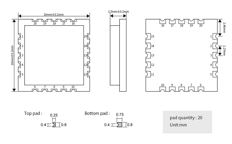
| 1.27mm | Stamp hole |
| Communication interface | SPI | 0-10Mbps |
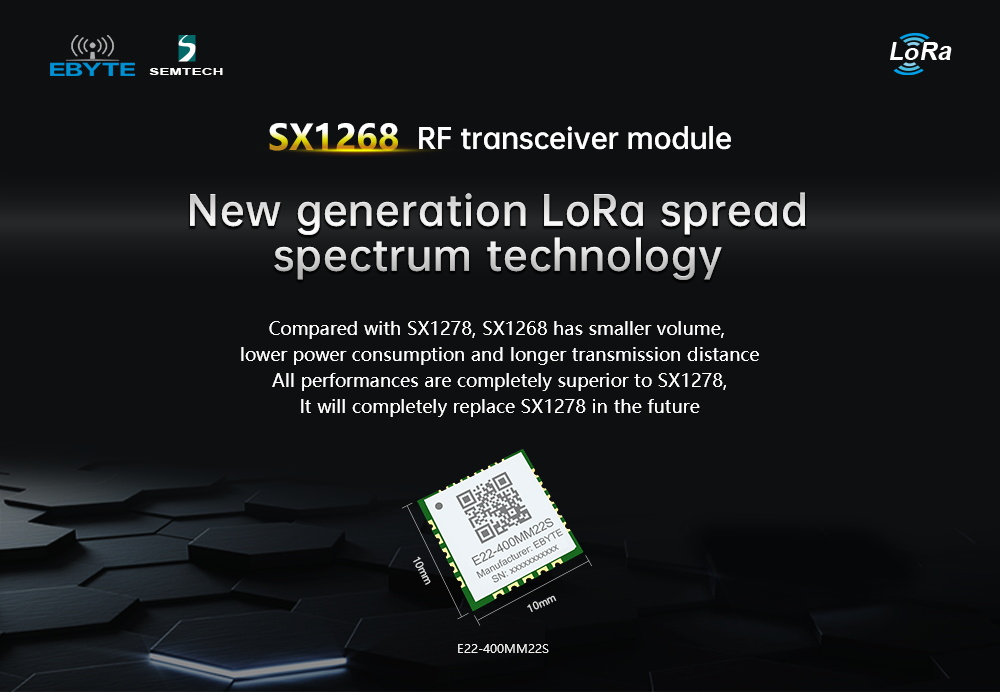
| Overall dimensions | 10* 10*2.5 mm | - |
| Antenna interface | Stamp hole/IPEX
| The equivalent impedance is about 50 ohms |
| mainly parameters | Performance | Notes |
Min
| Max |
| Power Supply Voltage(V) | 0 | 3.7 | Permanently burn module over 3.7V |
| Blocking power(dBm) | - | 10 | At close range, the burn
probability is low |
| Operating temperature(°C) | -40 | 85 | - |
| Product net weight | 0.5g士0.02g | Product net weight |

Pin number
| Pin name | Pin direction | Pin purposes |
| 1 | VCC | - | Power supply, range 1.8V~3.7V (external ceramic filter capacitor is recommended) |
| 2 | GND | - | Ground wire, connected to the power reference ground |
| 3 | NRST | input | Chip reset triggers input pin, active low level |
| 4 | NC
| - | - |
| 5 | NC | - | - |
| 6 | ANT | - | Radio frequency interface, stamp hole |
| 7 | GND | - | Ground wire, connected to the power reference ground |
| 8 | NC | - | - |
| 9 | TXEN | input | Rf switch transmitting control pin, connected to external
microcontroller IO or DIO2, high level effective |
| 10 | RXEN | input | Rf switch receiving control pin, connected to external
microcontroller IO, high level effective |
| 11 | BUSY | output | Used for status indication |
| 12 | MIS0 | output | SPI data output pin |
| 13 | M0SI | input | SPI data input pin |
| 14 | NSS | input | The module chip selection pin is used to start an SPI
communication |
| 15 | SCK | input | SPI clock input pin |
| 16 | GND | - | Ground wire, connected to the power reference ground |
| 17 | NC | - | - |
| 18 | DI03 | Input/output
| Configurable universal I/O port |
| 19 | DIO2 | Input/output
| Configurable universal I/O port |
| 20 | DI01 | Input/output
| Configurable universal I/O port |


