| Hardware Parameters | Parameter Value | Remark |
| Crystal oscillation frequency | 32MHz
| - |
Package -
| SMD | - |
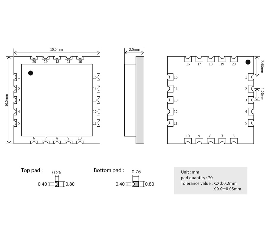
| Connector | stamp hole | Spacing 1.27mm |
| Communication interface | SPI
| 0-10Mbps |
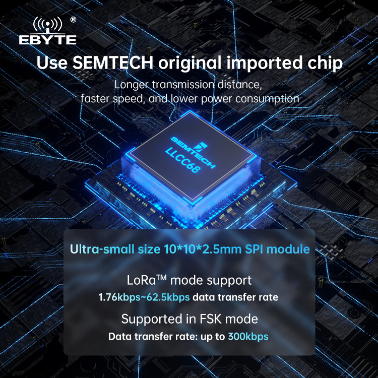
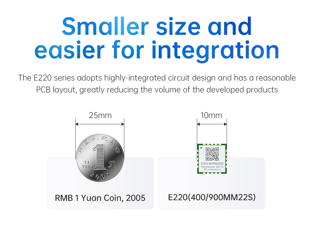
| Size | 10* 10*2.5 mm
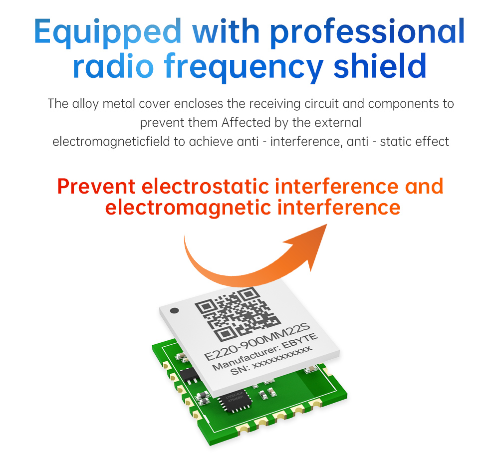
| With shield |
| Net weight | 0.5g±0.02g
|
|
| RF interface | stamp hole | - |
| Main Parameter | Performance | Remark |
| Min. | Type | Max. |
Operating voltage(V)
| 1.8 | 3.3 | 3.7 | ≥3.3V can guarantee the output power, more than 3.7V will permanently burn the module |
| Communication level(V) | - | 3.3 | - | Risk of burnout with 5V TTL |
| Operating temperature(°C) | -40 |
| +85 | Industrial grade design |
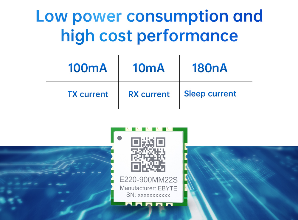
| power consumption | TX current
(mA) | - | 100 | - | Instantaneous power consumption |
RX current
(mA) | - | 10 | - | - |
Sleep current
(uA) | - | 1.2 | - | software shutdown |
| RF Parameter | Parameter Value
| Remark |
Operating frequency
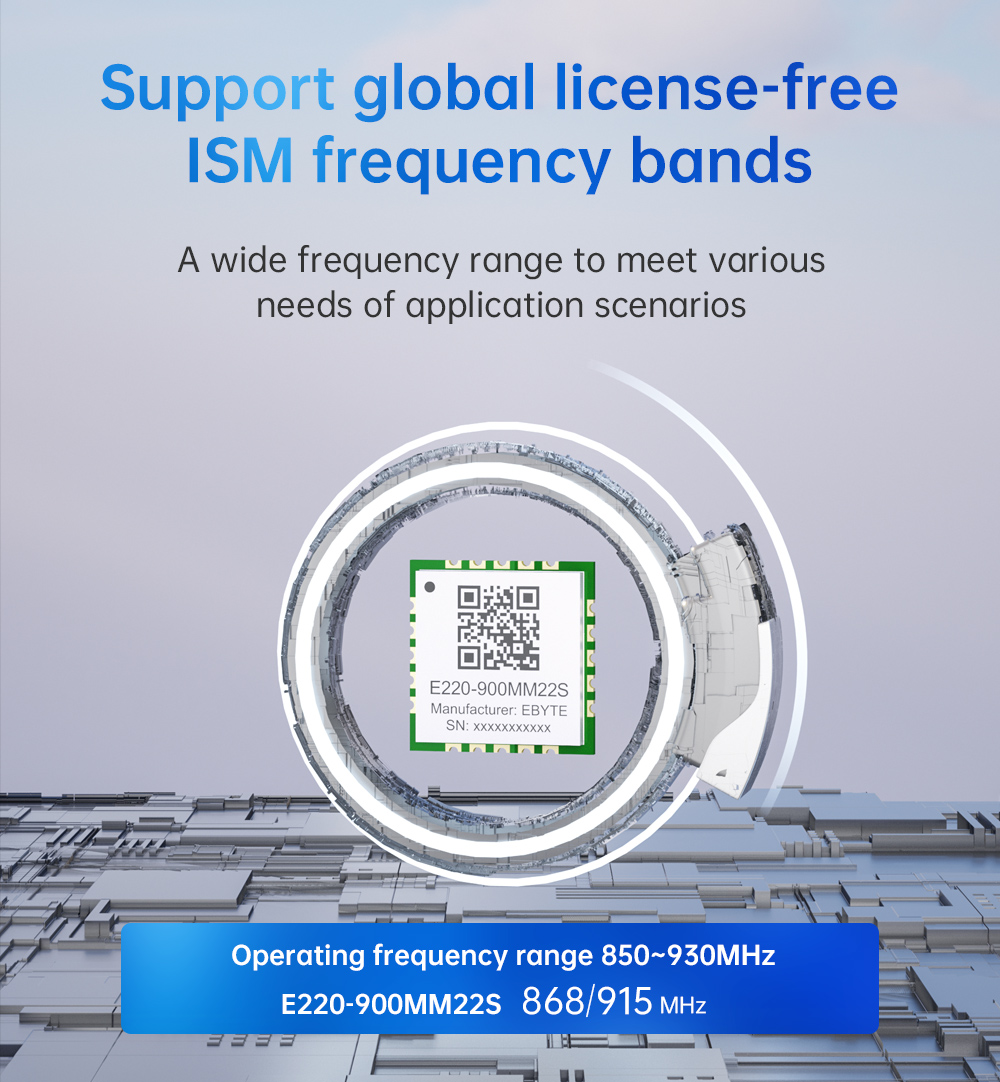
| 850MHz~930MHz
| Support ISM |
Transmit power
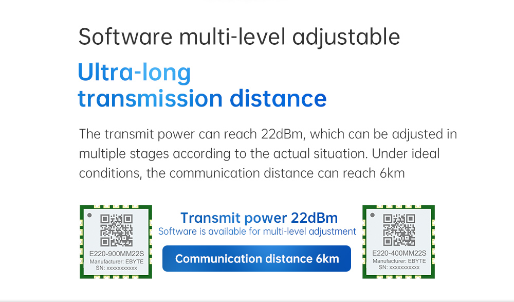
| 21dBm~22dBm
| The software is adjustable and needs to be developed and set by
the user |
| Receiving sensitivity | -129dBm
| BW_L=250kHz,SF = 10,LORATM |
FIFO
| 256Byte
| Maximum length of single transmission |
| Modulation mode LoRa | LoRa
| LoRa modulation is recommended |
| Blocking power | 10dBm
| The probability of burning at close range is small |
| Air rate LoRa | LoRa(bps) | 1.76k~62.5k
| User programming control |
| Reference distance | 5500m
| Clear and open environment, antenna gain 5dBi, antenna height
2.5 meters, air rate 2.4kbps |

| Pin No. | Item
| Direction | Description
|
| 1 | VCC | - | Power supply, range 1.8V~3.7V (recommended to add external ceramic filter capacitor) |
| 2 | GND | -
| Ground wire, connected to the power reference ground |
| 3 | NRST | Input
| NRST Input Chip reset trigger input pin, active low |
| 4 | NC | -
| -
|
| 5 | NC
| - | -
|
| 6 | ANT
| -
| RF interface, stamp hole |
| 7 | GND
| -
| Ground wire, connected to the power reference ground |
| 8 | NC
| -
| -
|
| 9 | TXEN
| Input | RF switch launch control pin, connected to external microcontroller IO
or DIO2, active high |
| 10 | RXEN
| Input | RF switch receiving control pin, connected to external microcontroller
IO, active high |
| 11 | BUSY | Output | Used for status indication (see LLCC68 manual for details) |
| 12 | MISO
| Output | SPI data output pin |
| 13 | MOSI
| Input | SPI data input pin |
| 14 | NSS
| Input | Module chip select pin for starting an SPI communication |
| 15 | SCK
| Input | SPI clock input pin |
| 16 | GND
| -
| Ground wire, connected to the power reference ground |
| 17 | NC
| -
| -
|
| 18 | DIO3
| Input/Output | Configurable general-purpose IO port (see LLCC68 manual for details) |
| 19 | DIO2
| Input/Output | Configurable general-purpose IO port (see LLCC68 manual for details) |
| 20 | DIO1 | Input/Output | Configurable general-purpose IO port (see LLCC68 manual for details)
|


